


● Applicable for the 6-inch, 8-inch and 12-inch wafer marking.
● With UV laser, the focusing spot is fine, and it is non-contact marking.
● Fully-automatic loading and unloading, automatic edge searching, simple operation and high efficiency.
● The whole system adopts computer control, Windows operation platform,interface in English, self-developed software, easy to operate.
● With high automation, it has the function of automatic fault alarm.
● Precise marking to the product DIE.
Features
Wafer Laser Processing – Wafer Marking/Etching
- Automatic wafer pick-up from the magazine
- Finding wafers automatically with edge seeker
- Automatic positioning marking with the visual system
- The visual inspection system is available
- Available to mark on the backside of the wafer through the transmittance film
- Complies with the SMEMA standard
- SMIF and other automatic loading and unloading modules can be selected as an extension
- UV and Green laser modules can be selected upon to the demand
Wafer Laser Processing – Silicon Wafer Dicing and Scribing
- Laser dicing of materials such as Si, SiC, SiO, GaN, etc
- Equipped with robotic arms, calibrators, and an automatic ring cleaning structure for fully automated production, effectively improving efficiency
- Compatible with 6-inch and 8-inch wafer
- The cutting effect has a small heat-affected zone and minimal chipping
- Cutting speed exceeds 100 mm/s, cutting depth exceeds 50 μm, and cutting line width exceeds 10 μm
- UV and Green laser can be selected upon to the demand
Application and Samples
6-inch, 8-inch, 12-inch wafer front or back marking


Technical Specs
| Laser Type | UV Laser |
| Wavelength | 355 nm |
| Min Beam Diameter | <10µm |
| Beam Quality M2 | < 1.2 |
| Pulse Frequency | 10 – 200 kHz |
| Output Power | 10 Watts |
| Repetition Accuracy | 2 μm |
| Cooling System | Water-cooled |
| Fθ Marking Field Size | 1.96″ x 1.96″ (50mm x 50mm) |
| X, Y travel Distance | 15.74″ x 11.81″ (400mm x 300 mm) |
| Laser Safety Level | Class I |
| Electrical Connection | 110 – 230 V (± 10%) 20 A, 50/60 Hz |
| Power Consumed | 5 Kw |
| Warranty Coverage | 1-year |
| Laser Safety Compliance | FDA(CDRH) |
| Running Temperature | 15℃-35℃ / 59°-95°F |
Options and Accessories
SMIF, other automatic loading and unloading modules

Robotic Arm

Calibrator

Smoke Purifier
Related Products

Mainly designed to mark and verify the ECC200 data matrix and other bar codes, batch numbers, and logos.

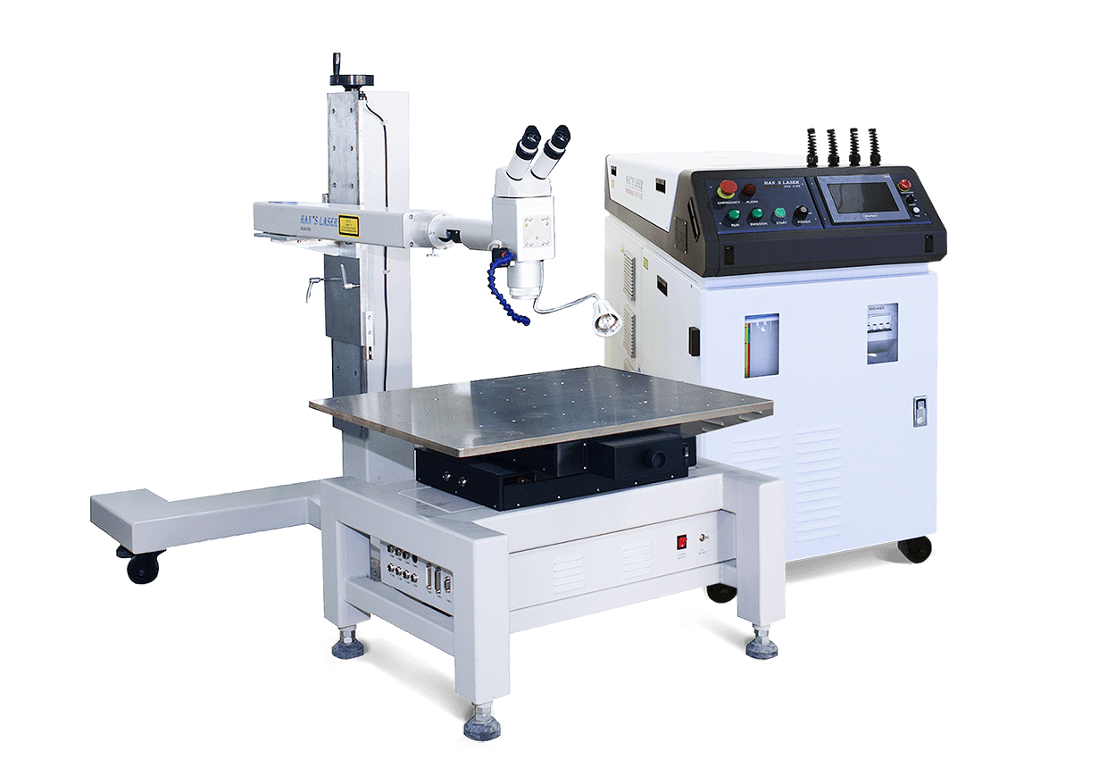
Ideal for stainless sheet, iron sheet, galvanized sheet as well as aluminum sheet welding.
Can be used to repair cracks, chippings, edges and corners, sand holes and mold wear after use.

Suitable for rigid and flexible substrate cutting and marking, like FR4 substrates and imitation…