Semiconductor manufacturing is an intricate process that involves multiple steps, each of which must be carried out with precision and accuracy to ensure the final product meets the highest quality standards. One of the key challenges in this process is identifying individual wafers and tracking them throughout the production cycle.
Traditionally, wafers have been marked manually with a unique identifier, such as a barcode or serial number. However, this method is time-consuming, labor-intensive, and prone to human error, which can result in misidentification, misplacement, or misinterpretation of the data.
To address this challenge, Han’s Laser has developed the fully automatic wafer edge ID marking system. This cutting-edge technology uses advanced imaging technology to scan the edges of wafers and then apply a unique identifier to each one automatically.
The system is highly efficient, with the ability to mark up to 120 wafers per minute, making it an ideal solution for high-volume production environments. It also offers a high degree of accuracy and consistency, reducing the risk of human error and ensuring that the wafers are correctly identified and tracked throughout the production cycle.
One of the key advantages of the wafer laser marking system is its flexibility. The system can be customized to mark wafers with a wide range of identifiers, including barcodes, 2D codes, and custom markings. This means that semiconductor manufacturers can choose the identification method that best suits their needs and integrate the system seamlessly into their existing production processes.

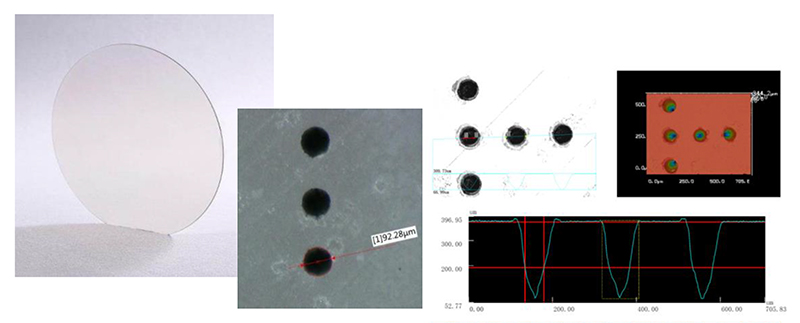
Si wafer, soft marking: spot diameter 52um; depth 1.5um
Another advantage of the system is its ease of use. The system can be operated by a single operator, who simply needs to load the wafers onto the system and press a button to start the marking process. The system also features a user-friendly interface that allows operators to monitor the marking process and track the status of each wafer in real-time.
In addition to its efficiency and ease of use, the wafer edge ID laser marking machine also offers a high degree of reliability. The system is designed to operate continuously without interruption, and it includes multiple safety features to prevent damage to the wafers or the system itself.

SiC wafer, hard marking: spot diameter 90um; depth 300um
Overall, the fully automatic wafer edge ID laser marking system is a highly advanced and effective solution for wafer identification and tracking in semiconductor manufacturing. It offers a range of benefits, including increased efficiency, accuracy, and reliability, while also being flexible and easy to use. As such, it represents a significant step forward in the world of semiconductor manufacturing and is likely to become an essential component of many high-volume production processes in the years to come.

